![]()
|
|
|
Projection Photolithography by Masud Mansuripur and Rongguang Liang
Photolithography is the technology of reproducing patterns using light. Developed originally for reproducing engravings and photographs, and later used to make printing plates, photolithography was found ideal in the 1960s for mass-producing integrated circuits.1 Projection exposure tools, which are now used routinely in the semiconductor industry, have continually improved over the past several decades to satisfy the insatiable demand for reduced feature size, increased chip size, improved reliability and production yield, and lower overall cost. High numerical aperture lenses, short-wavelength light sources, and complex photoresist chemistry have been developed to achieve fabrication of fine patterns over fairly large areas. Research and development efforts in recent years have been directed at improving the resolution and depth of focus of the photolithographic process by using phase-shifting masks (PSMs) in place of the conventional binary intensity masks (BIMs). In this article we describe briefly the principles of projection photolitho-graphy and explore the range of possibilities opened up by the introduction of PSMs.
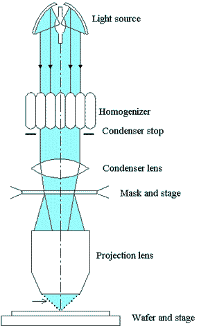
Basic principles. Figure 1 is a diagram of a typical projection system used in optical lithography. A quasi-monochromatic, spatially incoherent light source (wavelength = l) is used to illuminate the mask. Steps are usually taken to homogenize the source, thus ensuring a highly uniform intensity distribution at the plane of the mask. The condenser stop may be controlled to adjust the degree of coherence of the illuminating beam; this control of partial coherence is especially important when PSMs are used to improve the performance of optical lithography beyond what is achievable with the traditional BIMs.
Figure 1. Essential elements of a photolithographic �stepper� used for exposing semiconductor wafers. The condenser stop controls the degree of coherence of the illumination. The numerical aperture NAo of the projection lens is defined as sin q, where q is the half-angle of the cone subtended by the clear aperture of the projection lens at the wafer. The uniformly illuminated mask is imaged onto the wafer with a magnification M that is typically around 1/5. (Adopted from [1].)
The light transmitted through the mask is collected by the projection lens, which images the mask onto the wafer, typically with a magnification of M = 1/5. Thus, if the numerical aperture of the projection lens is defined as NAo = sin q, its angular aperture on the mask side will be sin q� = M NAo. If the condenser�s numerical aperture NAc happens to be much less than sin q�, the illumination is coherent, while if NAc � sin q� the illumination is essentially incoherent. In practice the ratio s = NAc/(M NAo) is used as a measure of the incoherence of illumination. For example, if M =1/5 and NAo = 0.6, then NAc = 0.084 yields s = 0.7, while NAc = 0.06 yields s = 0.5. For a given projection lens, therefore, the incoherence of illumination is proportional to the condenser stop diameter.1-3
Over the past decade photolithographic systems have evolved through several generations. The wavelength of the light source has steadily decreased from 365 nm (i-line of mercury) to 257 nm (high-pressure mercury arc lamp) to 248 nm (KrF laser), and is presently at 193 nm (ArF excimer laser). The numerical aperture NAo of the projection lens, having increased from its value of ~ 0.16 in the early days to ~ 0.6 in present-day systems, is likely to increase still further. The illumination systems have also improved, taking advantage of off-axis illumination and related configurations.1,2 Other improvements have occurred in the area of photoresists and control of their exposure and development processes, control of flatness of the wafer which reduces the need for a large depth of focus, etc. These topics are beyond the scope of the present article, and we refer the interested reader to the published literature for further information.1-6 In the remainder of this column we present computed images of various masks obtained in a typical projection system (NAo = 0.6, M = 1/5) and compare the resulting image contrasts and resolutions.
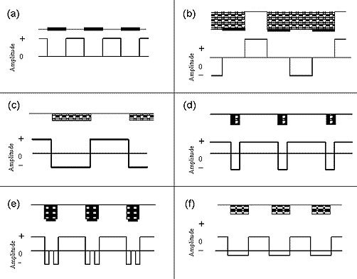
PSM versus BIM. Traditional �binary intensity� masks (BIMs) consist of opaque chromium lines on transparent glass substrates; these masks modulate the intensity of the incident light without affecting its phase. Modern masks have begun to take advantage of optical phase by changing the thickness of the transparent regions of the mask, either by depositing additional transparent material where needed, or by removing a thin layer from the substrate at specific locations, thereby selectively adjusting the transmitted optical phase.1,2 The basic idea of an optical phase-shifting-mask for lithography originated in the early 1980�s with M. D. Levenson6 in the U.S. and, independently and almost simultaneously, with M. Shibuya7 in Japan. Figure 2 shows a few different mask designs that exploit optical phase to improve the resolution of the photolithographic process. In addition to improved resolution, these PSMs also increase the effective depth of focus and provide a wider process window (i.e., range of acceptable focuses and exposures).1
Figure 2. Several mask structures and their corresponding E-field patterns immediately after transmission through the mask. (a) Conventional transmission mask. (b) Alternating aperture phase-mask with etched substrate. (c) Chromeless phase-edge mask produces dark lines in the image solely through destructive interference at the phase transitions. (d) Shifter-shutter mask is similar to (c) except that each dark line is produced by a pair of adjacent phase-edges. (e) Rim-shifter mask contains chrome lines bracketed by 180� phase-edges. (f) Attenuated phase-shift mask; here the shaded regions represent partially transmissive material with a 180� phase shift. (Adopted from [1].)
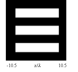
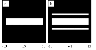
Alternating aperture phase-shifting mask. Consider the simple mask consisting of three bright lines on a dark background shown in Figure 3. Each bright line is 3l-wide, and the separation between adjacent lines is also 3l. (Note that these are the mask dimensions; at the wafer the features are demagnified by a factor of 1/M = 5.) We assume two different designs for the mask. In the first instance the mask is a conventional BIM, with the same phase imparted to the light transmitted through each aperture. In the second case we consider a PSM in which the upper and lower bright lines are phase-shifted by 180� relative to the central bright line.
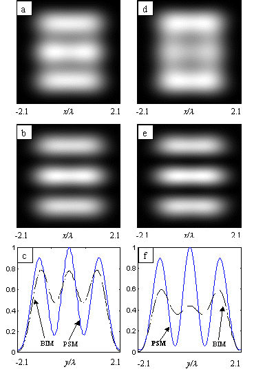
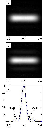
Figure 3. A simple mask containing three transparent apertures on an opaque background. The apertures as well as the spaces between apertures are 3l-wide. When the apertures impart a uniform phase to the transmitted beam, the mask is a BIM. When the upper and lower apertures impose on the transmitted beam a 180� phase-shift relative to the middle aperture, the mask is an alternating-aperture PSM . In Figures 4(a) and 4(b) we compare the intensity patterns of the images obtained at the wafer for these two types of mask. The assumed projection system is that of Figure 1 with NAo = 0.6, M = 1/5, and s = 0.7. Clearly the PSM is better at resolving the dark spaces between adjacent bright lines. For direct comparison, a cross-section through these two intensity distributions is shown in Figure 4(c). Increasing the coherence of illumination by closing down the aperture of the condenser to s = 0.5 improves the image contrast of the PSM but degrades that of the BIM image, as can be readily observed in Figures 4(d)-(f).8
Figure 4. Computed plots of intensity distribution at the wafer for the mask of Figure 3 placed in the system of Figure 1 (NAo = 0.6, M = 1/5). (a) Image of the BIM obtained with s = 0.7. (b) Image of the PSM obtained with s = 0.7. (c) Cross sections of the intensity patterns for the BIM (dashed) and the PSM (solid). (d)-(f) Same as the patterns in the left-hand column, but for s = 0.5.
Isolated bright line. As our second example we consider the case of an isolated bright line. Figures 5(a) and 5(b) show respectively a BIM and a PSM for a line of width 4l. (Again, this is the dimension at the mask; the projected line at the wafer is only 0.8l-wide.) The PSM of Figure 5(b) contains two 0.8l-wide side-riggers, each imparting a 180� phase-shift to the incident beam relative to the central bright line.4 Figures 6(a) and 6(b) show the computed intensity patterns at the wafer for the two masks, and Figure 6(c) shows cross-sections of both patterns (assumed coherence factor s = 0.7).8 The side-riggers produce small bumps in the intensity pattern of the PSM, but these are usually below the resist threshold and are not printed. In Figure 6 the computed image of the bright line using the PSM is about 10% narrower than that obtained with the BIM. This modest reduction in the printed line-width can be slightly improved upon if the side-riggers location and width are properly optimized and also if the condenser stop is further closed down to increase the coherence of illumination. (s values as low as 0.3 have been suggested in the literature.4,5)
Figure 5. Masks designed for creating an isolated bright line at the wafer. (a) BIM containing a 4l-wide line on an opaque background. (b) PSM featuring the same 4l-wide line flanked by a pair of 0.8l-wide side-riggers. Each side-rigger imparts to the incident beam a 180� phase-shift relative to the central line. The separation between the central line and each side-rigger is 2l.
Figure 6. Computed intensity patterns at the wafer for the masks of Figure 5 in the system of Figure 1 (NAo = 0.6, M = 1/5, s = 0.7). (a) BIM, (b) PSM, (c) cross-sections of the intensity patterns in the images of the BIM (dashed) and the PSM (solid).
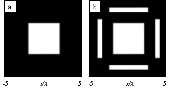
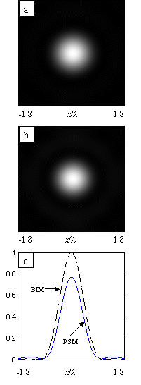
Contact hole. Figure 7(a) shows a simple, 4l � 4l square aperture on a dark background. This feature has uniform phase across the aperture and, therefore, represents a BIM for a contact hole. A corresponding PSM for the same hole is shown in Figure 7(b). Here four side-rigger lines of width 0.5l and 180� phase-shift (relative to the central aperture) are placed around the hole.4 The computed intensity patterns of the images of these masks at the wafer appear in Figures 8(a) and 8(b), respectively. The side-rigger features are too small to be printed, but their destructive interference with the central aperture results in a smaller projected hole, as revealed in the cross-sectional intensity profiles at the wafer shown in Figure 8(c). As before, the printed feature size can be further optimized by adjusting the dimensions of the side-riggers as well as closing the condenser stop to reduce the value of s.
Figure 7. Mask patterns for creating a contact hole. (a) BIM containing a 4l � 4l square aperture on an opaque background. (b) PSM featuring the same 4l � 4l aperture surrounded by 0.5l-wide side-riggers. Each side-rigger imparts to the incident beam a 180� phase-shift relative to the central aperture.
Figure 8. Computed intensity patterns at the wafer for the masks of Figure 7 in the system of Figure 1 (NAo = 0.6, M = 1/5, s = 0.7). (a) BIM, (b) PSM, (c) cross-sections of the intensity patterns in the images of the BIM (dashed) and the PSM (solid).
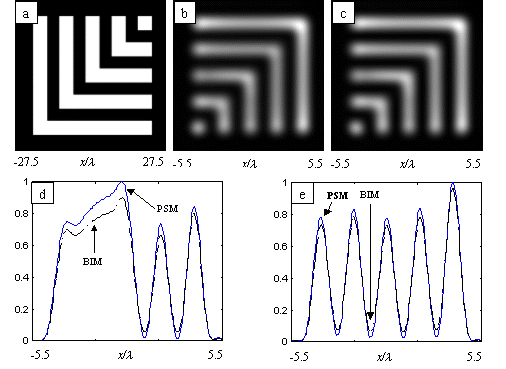
More complicated patterns. Figure 9(a) shows a mask with five transparent apertures. The widths of line (bright) and space (dark) on this mask are both equal to 4.8l. If the mask is used without any phase-shifts, the intensity pattern of Figure 9(b) will be obtained at the wafer. Placing 180� phase-shifters on alternate bright apertures results in the image intensity distribution shown in Figure 9(c). Two different cross-sections of these patterns are also given in Figures 9(d) and 9(e). In this case of relatively large features, there are apparently no significant differences between a BIM and a PSM.
Figure 9. (a) Mask pattern containing five transparent apertures on an opaque background. The lines and spaces are all 4.8l-wide. When assumed to be a BIM, all apertures impart the same uniform phase to the incident beam. When used as a PSM, the apertures are alternately phase-shifted by 0� and 180�. The assumed projection system parameters are NAo = 0.6, M = 1/5, s = 0.7. (b) Computed intensity pattern in the image of the BIM. (c) Computed intensity pattern in the image of the PSM; the arrows mark the cross-sections displayed in (d) and (e). (d) Cross-sectional plots of intensity distributions in the images of the BIM (dashed) and the PSM (solid). (e) A different cross-section of the two images.
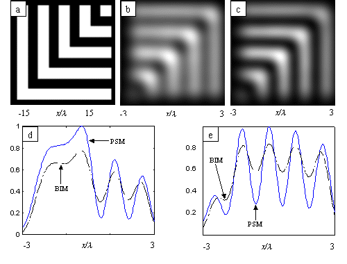
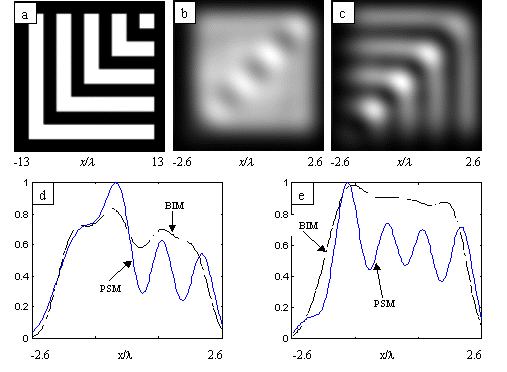
With shrinking features, however, the advantages of the PSM become apparent. Figure 10 is the counterpart of Figure 9 for the case where the line- and space-widths (at the mask) are both reduced to 3l. The BIM is now seen to yield a fairly low-contrast image at the wafer, while the PSM provides better resolution and sharper contrast. Reducing the feature size still further to 2.4l (at the mask) results in the patterns of Figure 11. Here the PSM still performs reasonably well, while the image quality of the BIM has substantially degraded.
Figure 10. Same as Figure 9 but for smaller mask features. The lines and spaces on the mask are now 3l-wide.
Figure 11. Same as Figure 9 but for very small mask features. The lines and spaces on the mask are now 2.4l-wide.
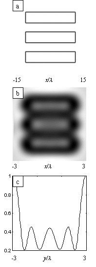
Phase-shifters on a transparent background. As a final example, consider the fully transparent (i.e., chromeless) PSM shown in Figure 12(a). Each of the three rectangular features on this mask is 4l-wide and is phase-shifted by 180� relative to the background. Also, the spaces separating adjacent rectangular features are each 4l-wide. The computed intensity distribution at the wafer in a system having NAo = 0.6, M = 1/5, s = 0.7 is shown in Figure 12(b), and a cross-sectional view is provided in Figure 12(c).8 Depending on the intended application, this image may or may not be acceptable. For instance, suppose the long edges of the rectangular features of the mask are meant to produce dark lines at the wafer. This they do quite well, as is evident from the presence of four horizontal dark lines in Figure 12(b). However, if the ends of these dark lines are required to be disconnected from each other, then the PSM has failed in providing the necessary isolation. The problem is rooted in the sharp 0�-180� phase-edge occurring at the short end of each rectangular feature. This problem can be remedied in principle by softening the phase transition at these short ends by providing a gradual transition from 180� to 120� to 60� and eventually to 0�. Such phase stair-steps, however, are usually impractical because they are costly and, moreover, they produce masks that are difficult to inspect and to repair. In today�s practice, such unwanted dark lines are erased by a second exposure through a different mask.
Figure 12. (a) Transparent PSM containing three rectangular regions of width 4l, each imparting a 180� phase-shift to the incident beam. Like the background, the spaces between adjacent apertures (also 4l-wide) are fully transparent and impart a 0� phase to the beam. (b) Computed intensity distribution in the image plane of the system of Figure 1 having NAo = 0.6, M = 1/5, s = 0.7. (c) Central cross-section of the intensity pattern of the image seen in (b).
Concluding remarks. Incorporating the advantages of optical phase in the design, manufacture, and testing of photomasks is still very much a research topic, with many potential benefits of the PSM remaining to be realized. The type of PSM in common use today is the attenuated PSM depicted in Figure 2(f), where the traditional opaque chrome is replaced by a material that transmits ~ 8% with a 180� phase shift. This is useful for printing bright spaces and contact holes, and has essentially replaced the shifter-shutter type of mask (see Figure 2(d)). Also, the more recent high-transmission tri-tone PSM, where the phase-shifted material transmits ~ 18% and there is a separately patterned opaque layer, has superceded the rim-shifters (see Figure 2(e)).9
Acknowledgements. The authors are grateful to Dr. Marc D. Levenson for illuminating discussions, and to Dr. Michael Descour of the Optical Sciences Center, University of Arizona, for criticism of an early draft of this article.
References1. M. D. Levenson, �Wavefront engineering for photolithography,� Physics Today, 28-36, July 1993. 2. M. D. Levenson, �Extending the lifetime of optical lithography technologies with wavefront engineering,� Jpn. J. Appl. Phys. 33, 6765-6773 (1994). 3. M. D. Levenson, �Wavefront engineering from 500 nm to 100 nm CD,� in Emerging Lithographic Technologies, SPIE Proc. Vol. 3048, 2-13 (1997). 4. T. Terasawa, N. Hasegawa, T. Kurosaki, and T. Tanaka, �0.3-micron optical lithography using a phase-shifting mask,� SPIE 1088, 25-33 (1989). 5. N. Hasegawa, T. Terasawa, T. Tanaka, and T. Kurosaki, �Submicron optical lithography using phase-shifting mask,� Electro-chem. and Ind. Phys. Chem. 58, 330-335 (1990). 6. M. D. Levenson, N. S. Viswanathan and R. A. Simpson, �Improving resolution in photolithography with a phase-shifting mask,� IEEE Transactions on Electron Devices, ED-29, 1828-1836 (1982). 7. M. Shibuya, �Projection master for transmitted illumination,� Japanese Patent Gazette # Showa 62-50811, application dated 9/30/80, issued 10/27/87. 8. The computer simulations reported in this article were performed by DIFFRACT�, a product of MM Research, Inc., Tucson, Arizona. 9. M. D. Levenson, private communication.
Home
| About MM Research, Inc. | Online
Publications © Copyright 1987-2011, MM Research, Inc. 5748 N. Camino del Conde, Tucson, Arizona 85718 |